
Chalcogenide Letters Vol. 20, No. 2, February 2023, p.113 - 120
Effect of phosphoric acid treatment on the physical properties
of zinc telluride thin films
A. K. Aqili
a,*
, T. Abu-Omar
a
, A. Y. Al-Reyahi
a
, A. Shaheen
a
, S. Al-Omari
a
,
I. Alhagish
a
a
Department of Physics, Faculty of Science, The Hashemite University, P.O. Box
330127, Zarqa, 13133 Jordan
Zinc Telluride (ZnTe) films were prepared by the closed space sublimation (CSS) method.
The effect of chemical treatments with concentrated phosphoric acid, on the optical,
electric and structural properties of the films was studied. Zinc-blend structure of the
polycrystalline nature of the films was confirmed by x-ray diffraction (XRD) spectra. The
energy dispersive x-ray (EDX) shows an increase in Te ratio on the surface of the film as
exposed to phosphoric acid. In addition, the dc electrical resistivity of the films was
dropped considerably. The refractive index, thickness, and thickness irregularity of the
films were determined by fitting of the optical transmittance spectra in the wavelength
range 400 to 2500 nm. The effect, of treatment, on the optical parameters is also reported.
(Received November 9, 2022; Accepted February 7, 2023)
Keywords: ZnTe, Thin films, Optical properties, X-ray diffraction, Zinc compound,
Semiconducting II-VI materials
1. Introduction
Polycrystalline compound semiconductors films of are considerable technological
importance and play a major role in electronic devices. ZnTe is one of the group II-VI
semiconductors having a wide range of applications such as green light emitting diodes [1,2] due
to its excellent electrical and optical properties. ZnTe is a p-type semiconductor with a direct band
gap of 2.26 eV and a zinc-blend structure [3,4]. In addition to that doped ZnTe is used as a buffer
layer, between CdTe absorber and metallic contact, in CdTe/CdS solar cells [5]. Due to importance
of ZnTe a variety of methods have been utilized for deposition including pulsed laser deposition
[1,5], sputtering [6,7], thermal evaporation [8–12], electron beam [13,14], screen printing [15],
electro-deposition [16], brush plated [17] and closed space sublimation [3,18–20]. It is obvious
that the deposition method and post-treatment have a great effect on the physical properties of the
films.
Among the deposition methods, the CSS method is an attractive method for the deposition
of II-VI semiconductor films. This is due to a good quality film that can be achieved under
moderate pressure [3] and comparatively fewer materials use. On the other hand, it was reported
that [21] treating CdTe (which has a similar structure as ZnTe) with nitric-phosphoric acid can
improve its electrical properties.
In this work, we prepared ZnTe films by closed space sublimation method and then
immersed them in concentrated phosphoric acid for different time periods. The effect of
immersion of these films, in phosphoric acid, on their optical, structural, and electrical properties
were studied.
2. Experimental
High-purity ZnTe powder (99.99) was used as source material for the deposition of the
films, by CSS method, on carefully cleaned ultra-white glass substrate. Detailed descriptions of the
*
Corresponding author: [email protected]
https://doi.org/10.15251/CL.2023.202.113
114
deposition unit are given in reference [20]. The distance between the source material and substrate
was fixed at 0.8 cm. After achieving a base pressure of 0.01 mbar the substrate temperature was
raised to 400
0
C and then the source temperature was gradually raised to 600
0
C and kept at this
temperature for 5 minutes. The source heater then turned off while the substrate was kept at the
same deposition temperature for 30 minutes before switching off the substrate heater and allowing
the system to cool down. Many films were deposited with the same parameters. After deposition,
the films were immersed in concentrated phosphoric acid, at 30
0
C, for different time periods as
listed in table 1, then rinsed with distilled water and dried with dry nitrogen.
The optical transmittance, in the wavelength range from 400 to 2500 was recorded by
Perkin -Elmer Lambda 19, UV-VIS-NIR spectrophotometer with UV-WinLab software. X-ray
diffraction patterns, with Cu-Kα radiation, were used to study the structure of the films. The
composition of the films was determined by energy dispersive system (EDS) attached to SEM. The
surface morphology of the films was studied by scanning electron microscopy (SEM). The
resistivity of the films was measured as function of temperature.
3. Results and discussion
3.1. Surface analysis and composition
The EDS results show that the tellurium ratio increased from 65 wt.% for as deposited
film to 69 wt.% for film immersed for 48 hours. The tellurium ratio in the films increases as
immersion time increases, which indicates the formation of a tellurium rich surface. The scanning
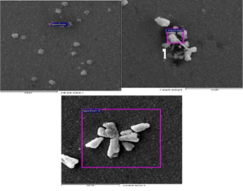
electron microscope images, as shown in Fig.1, show a smooth surface with randomly distributed
small spherical crystalline on the surface. This is due to that the film surfaces are dense, smooth,
and compact in nature. However, a higher density of crystallite structure appears in immersed
films. It could be explained in terms of surface etching, i.e., revealing the inner structure of the
film.
Fig. 1. Sem images of the films Z0 (left), Z24(middle), and Z48 (right).
115
3.2. Structural analysis
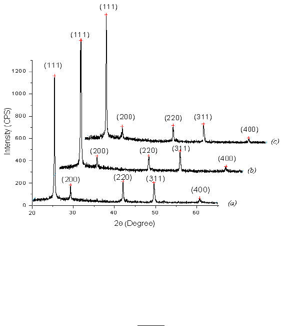
The x-ray diffraction patterns (Fig.2) show that all the ZnTe thin films (with or without
immersion in phosphoric acid) prepared at the same substrate temperature and having almost the
same thickness are present as a crystalline structure composed of cubic phase with a (111)
preferred orientation. This structure and preferred orientation are common for ZnTe films
deposited with a wide variety of techniques [1–12]. No notable changes in film structure or
orientation were observed after immersion in phosphoric acid as in Fig.2.
Compared with standard JCPDS card No.15-0746, all ZnTe films exhibit a zinc blend
structure with strong preferential (111) orientation. The (111) peak positions which are located at
2θ are 25.4198
0
, 25.3996
0
, 25.4196
0
, and 25.3991
0
for the films deposited at different immersion
times, respectively.
Fig. 2. Xrd pattern of the films Z0 (a), Z24(b) and Z48 (c).
The variation in crystalline size of the films was determined from the full width at half-
maximum (FWHM ) of the peak corresponding to the (111) plane using the Scherer relation [1,4]
=
0.94
where t is the diameter of the crystalline particle, λ is the wavelength of the x-ray used (0.154 nm),
B is the full width at half-maximum and θ is the scattering angle. The calculated crystalline size of
the films is ~ 45 nm and a slight difference (~ 2 nm) observed in the crystalline size could be
attributed to the small difference in the thickness of the film. The calculated crystalline size was
larger than that reported by other deposition methods [1].
3.3. Electrical properties
The P-type conductivity of the films were verified by a well-known hot probe method. The
room temperature resistivities for all films are listed in table 2. The resistivity of the as deposited
films was very high ~ 10
6
Ω-cm, which is close to that reported for undoped ZnTe [3] films.
However, the resistivity has been dropped to ~10
4
Ω- cm for treated films. With no available
literature related to the phosphoric acid treatment of ZnTe films (according to our knowledge), the
reduction of resistivity by etching CdTe by phosphoric acid was reported by reference [21]. They
reported that there is a decrease in the film’s resistivity and a reduction in the effective bulk
resistivity due to the formation of a Te-rich layer on the grain boundaries.
116
The linear relation between the current and voltage which confirm ohmic contact junction
with ZnTe film and silver paste used to measure the conductivity. Moreover, this linear relation
indicates ohmic contact between the film surface and metallic contact which could be useful for
the application of ZnTe as a buffer layer between CdTe absorption layer and metallic contact for
CdTe based solar cells.
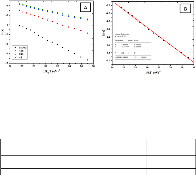
The dark conductivity activation energy (
=
−
) was obtained by linear fitting ln
σ vs. k
B
T, where k
B
is the Boltzmann constant, E
F
is the fermi energy level and E
V
is the energy at
the top of valance band. Fig. 3 shows the linear relation between ln σ and 1/k
B
T and the electrical
results are listed in Table1.
Fig. 3. plot of ln(σ) against 1/kT for all films (A).and Fitting of ln(σ) against 1/kT for film Z24 (B).
It clearly shows that the conductivity activation energy of the films was reduced from 0.64
eV to 0.26 eV indicating increase of hole concentration led to shift of fermi energy level closer to
the valence band.
Table 1. The dc electrical resistivity of the as deposited and immersed ZnTe films.
Film number
Immersion time (hour)
Activation Energy E
a
(eV)
Resistivity ρ (Ω.cm)
Z0
0
0.64
1.26 × 10
6
Z12
12
0.30
1.29 × 10
5
Z24
24
0.28
4.07 × 10
4
Z48
48
0.26
2.19 × 10
4
3.4. Optical properties
The as deposited zinc telluride films were orange in color. The films lose their
transparency as immersed in a phosphoric acid solution. This can be attributed to an increase in
tellurium on the surfaces of the films.
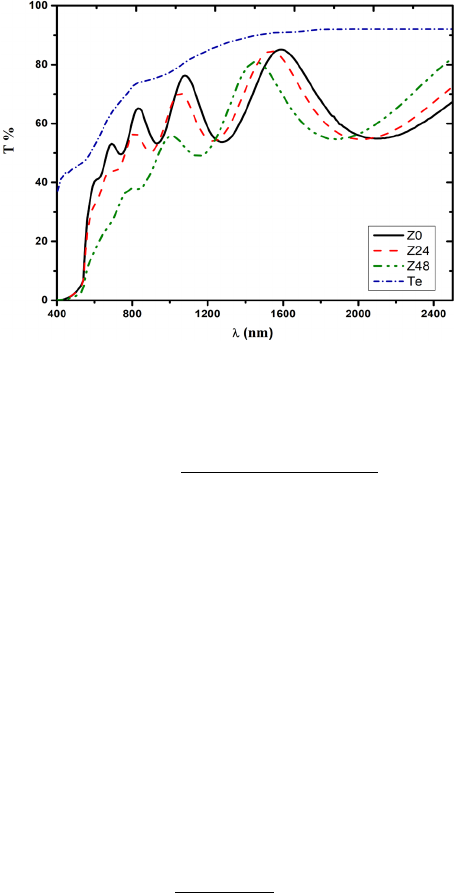
Fig. 4. shows the transmittance spectra of as deposited as well as treated films along with
transmittance spectra of 10 nm tellurium film, in order to compare the decrease of transmittance
due to the increase of Te concentration in the films. It is obvious that the reduction of
transmittance below 2000nm follows the same trend as tellurium film. The reduction of
transmittance is attributed to the formation of Te excess layer on the film surface due to etching
with phosphoric acid. The normal transmittance (T) for a system of thin film (of refractive index n
and extinction coefficient k) on a transparent substrate (of refractive index n
s
) surrounded by air
and k
2
<< n
2
can be written as [11,22]
117
Fig. 4. Transmittance of prepared ZnTe films along with 10 nm Te film.
2
)cos( Dx
CxB
Ax
T
+−
=
φ
(1)
2222
]))1()/2(5.0[(16 nnnExpA
s
−−=
λps
,
)()1(
23
s
nnnB ++=
,
]))/2(2[()()1(2
2222
2
2
nExpnnnC
s
λps
−−−=
22
2
223
]))/2
(2(exp[)()1( nnnnD
s
λps
−−−=
,
λpφ
/4 nd=
,
d
ex
α
−
=
.
λ
pα
/4
k=
Here, λ is the incident photon wavelength, d is the film thickness, φ is the phase angle, α
is the absorption coefficient and σ is the RMS height of surface roughness(irregularity). It was
found that the refractive index of the ZnTe films obeys the simple classical dispersion relation for
a single oscillator centered at wavelength λ
0
[11,12,22] and expressed by
2/1
2
0
2
22
0
)
)1(
1(
λ
λ
λ
−
−
+=
n
n
, (2)
where n
0
is the infinite wavelength refractive index. The wavelength dependence of the absorption
process is complicated, resulting from impurity, defects, or multi-phonon absorption [23].
Therefore, in case of low absorption coefficient, it may be expanded in a Taylor series around the
photon energy far from absorption line. If only terms up to second degree are included (α varies
slowly with λ), the relation for α can be expressed as:
)()/
/
(
2
λ
λλα
hlm
efgc
+
+++=
, (3)
118
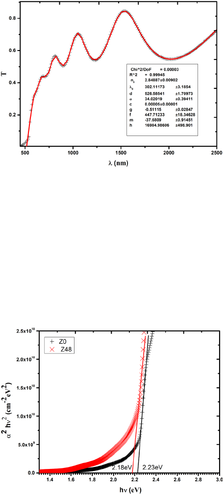
Fig. 5. Transmittance data of film Z24 along with fitting curve.
where c, g, f, m and h are fitting parameters. The second term in equation 3 is relating to Urbach’s
relation [24], which represents the absorption edge of an intrinsic semiconductor. While the first
term is a polynomial approximation of the absorption coefficient resulting from impurity, defects,
or multi-phonon absorption. Fig. 5 shows a good fitting in transparent and low absorption of
wavelength region, using equation 1 and substitution equations 2 and 3 for n and α. consequently,
the values of the thickness, thickness irregularity, and refractive index were obtained. However,
the values of the absorption coefficient in the high absorption region were found by solving
equation 1 after substituting the other parameters obtained from transmittance curve fitting.
Fig.6. Plot of α
2
(h
ν
)
2
against photon energy(h
ν
) for films Z0 and Z48.
For allowed direct transition, α varies with photon energy (h
ν
) as the well-known
dependence
α
~(h
ν
-E
g
)
1/2
. Near the absorption edge, the optical energy gap (E
g
) is obtained by
extrapolating (
α
)
2
against the photon energy plot as in Fig.6. The fitting results along with optical
energy gaps are listed in Table 2. No significant change in the surface roughness, which indicates
that deposition conditions are more dominant and effective in films morphology rather than post-
treatment and since all the films were prepared with the same deposition parameters there is no
clear difference in surface roughness and the roughness is comparable with grain size deduced
from x-ray results. The change in refractive index was clear as result of increasing in the films
absorption. Furthermore, minor shift of optical energy gap was observed.

119
Table 2. Fitting results along with calculated optical band gap.
Film
number
Thickness
d (nm)
Thickness
irregularity (nm)
Refractive index
Optical band
gap E
g
(eV)
n
0
λ
0
(nm)
Z0
563
29.3
2.77
288
2.23
Z12
420
28.6
2.70
330
2.22
Z24
526
34
2.82
302
2.20
Z48
500
31
2.83
293
2.18
4. Conclusions
Optical, electrical, and composition results insure the formation of Te rich layer by
immersion ZnTe films in concentrated phosphoric acid solution at room temperature. The
formation of Te rich surface led to increase the electrical conductivity of the films. No significant
change in the structure of the film was observed, while the optical properties such as refractive
index and optical energy band was slightly affected. The etching procedure was very slow, so it
required a long time for small changes in the physical properties to be observed. The Increase of
electrical conductivity with no drastic change in optical and structure of the films can attribute to
application where heavily doped zinc telluride layer is required.
References
[1] A. Erlacher, A. R. Lukaszew, H. Jaeger, B. Ullrich. Surface Science 600, 3762 (2006);
https://doi.org/10.1016/j.susc.2006.02.061
[2] F. J. Ochoa-Estrella, A. Vera-Marquina, I. Mejia, A. L. Leal-Cruz, M. Quevedo-López. J Mater
Sci: Mater Electron. 29, 7629 (2018); https://doi.org/10.1007/s10854-018-8755-3
[3] F. J. Ochoa-Estrella,A. Vera-Marquina, I. Mejia, A. L. Leal-Cruz, M. I. Pintor-Monroy M.
Quevedo-López. J Mater Sci: Mater Electron. 29, 20623 (2018);
https://doi.org/10.1007/s10854-018-0200-0
[4] H. Singh, T. Singh, J. Sharma. ISSS J Micro Smart Syst. 7, 123 (2018);
https://doi.org/10.1007/s41683-018-0026-2
[5] L. Feng, L. Wu, Z. Lei, W. Li, Y. Cai, W. Cai, J. Zhang, Q. Luo, B. Li, J. Zheng. Thin Solid
Films 515, 5792 (2007); https://doi.org/10.1016/j.tsf.2006.12.122
[6] E. A. Rakhshani, S. Thomas. J Mater Sci . 48, 6386 (2013);
https://doi.org/10.1007/s10853-013-7438-y
[7] H. Bellakhder, A. Outzourhit, E.L Ameziane. Thin Solid Films. 382, 30 (2001);
https://doi.org/10.1016/S0040-6090(00)01697-7
[8] H. Singh, P. Singh, A. Thakur, T. Singh, J. Sharma. Materials Science in Semiconductor
Processing. 75, 276 (2018); https://doi.org/10.1016/j.mssp.2017.12.002
[9] E. Bacaksız, S. Aksu, N. Ozer, M. Tomakin, A. Ozcelik. Applied Surface Science. 256, 1566
(2009); https://doi.org/10.1016/j.apsusc.2009.09.023
[10] S. Jeetendra, C. S. Naveen, P. Raghu, H. M. Mahesh. International Journal of Engineering
Research & Technology. 3, 431 ( 2014).
[11] A.K. S. Aqili, Z. Ali, A. Maqsood. Journal of Crystal Growth. 317, 47 (2011);
https://doi.org/10.1016/j.jcrysgro.2010.12.072
[12] A.K. S. Aqili, Z. Ali, A. Maqsood. Applied Surface Science. 167, 1 (2000);
https://doi.org/10.1016/S0169-4332(00)00498-0
[13] S. Jeetendra, H. Nagabhushana, K. Mrudula, C.S. Naveen, P. Raghu, H. M. Mahesh. Int. J.
Electrochem. Sci. 9, 2944 (2014).
[14] A. M..Salem, T. M. Dahy, Y. A. El-Gendy. Physica B: Condensed Matter 403, 3027 (2008);
https://doi.org/10.1016/j.physb.2008.03.005

120
[15] V. Kumar, V. Kumar, D. K. Dwivedi, (2012). Physica Scripta. 86, 015604 (2012);
https://doi.org/10.1088/0031-8949/86/01/015604
[16] A.B.M.O. Islam, N.B. Chaure, J.Wellings, G.Tolan, I.M.Dharmadasa. Materials
Characterization. 60, 160 (2009); https://doi.org/10.1016/j.matchar.2008.07.009
[17] K. R. Murali, M. Ziaudeen, N. Jayaprakash. Solid-State Electronics 50, 1692 (2006);
https://doi.org/10.1016/j.sse.2006.09.003
[18] W. Mahmood, S. Awan, A. Ud Din, J. Ali, M. F. Nasir, N. Ali, A. Haq, M. Kamran, B.
Parveen, M. Rafiq, N. A. Shah. Materials (Basel).12, 1359 (2019);
https://doi.org/10.3390/ma12081359
[19] w. Mahmood, A. Thomas, A. ul Haq, N. A. Shah, M. F. Nasir. Journal of Physics D: Applied
Physics. 50, 255503 (2017); https://doi.org/10.1088/1361-6463/aa7157
[20] A. Aqili, A. J. Saleh, Z. Ali, Zulfiqar, S. Al-Omaria. Journal of Alloys and Compounds.
520,83 (2012); https://doi.org/10.1016/j.jallcom.2011.12.094
[21] X. Li, D. W. Niles, F. S. Hasoon, R. J. Matson, P. Sheldon. Journal of Vacuum Science &
Technology A. 17, 805 (1999); https://doi.org/10.1116/1.581651
[22] A. K. S. Aqili, Z. Ali, S. Al-Omari, F. Afaneh. Chalcogenide Letters. 15(9),467 (2018).
[23] A. Aqili, A. Maqsood, Z Ali. Applied Surface Science 191,280 (2002);
https://doi.org/10.1016/S0169-4332(02)00218-0
[24] A. Aqili, A.Maqsood, Applied optics. 41, 218 (2002);
https://doi.org/10.1364/AO.41.000218
